Interfacing materials. Interfacing disciplines.
Home | PI Info | Research | Publications | Mentoring/Outreach | Links

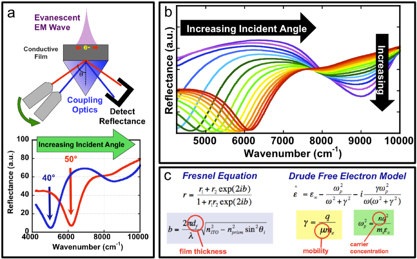
Surface plasmon resonance (SPR) is used to detect molecular species and to measure molecular binding kinetics at surfaces. The Kretschmann configuration depicted in Fig. 1a is commonly used to optically excite a surface plasmon polariton. The coupling optics enable proper matching of the light’s momentum vector to the plasmon. The SPP consists of a collective electronic oscillation coupled to an evanescent electromagnetic (EM) wave. At the proper combination of incident light wavelength and angle, the SPR is excited. At SPR, the reflectance goes down because the photon’s energy is being used to excite the plasmon. Because excitation requires momentum matching, changing the light’s angle of incidence shifts the plasmon’s resonance energy. The sensitivity of the evanescent EM wave to changes in the surface’s dielectric constant provides SPR with it’s ability to detect molecular binding events. Most SPR work has been done using noble metal thin films like Ag and Au that show SPR in the visible regime. We have conducted pioneering work in conductive oxides like indium tin oxide (ITO) that show SPR in the infrared. These systems offer a number of new opportunities such as the use of silicon-based IR optics and multiplexing with visible light characterization techniques, like fluorescence microscopy, that require a transparent substrate.
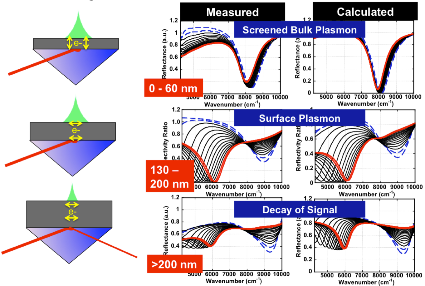
We have demonstrated SPR in ITO thin films and have developed theoretical calculations based on Fresnel reflection equations and the Drude free electron model that reasonably predicts plasmonic behavior without any fitting parameters. Unlike noble metal systems, we have found it possible to easily manipulate the SPR in conductive oxide thin films by adjusting structural features like film thickness, electronic carrier concentration, and electronic mobility. These capabilities are partially due to our exquisite control of ITO microstructure. Fig. 2 shows how film thickness changes the plasmon mode that is excited. For thin films (< 60 nm) we observe an excitation akin to the localized surface plasmon resonance seen in nanoparticles. We have also controlled defect density and microstructure to shift the SPR frequency and bandwidth (See Ref. 2 for more details).
Fig. 1: Surface plasmon resonance in conductive oxide thin films. (a) Kretschmann geometry (top) for excitation of SPR and reflectance spectra (below) showing how the resonance energy shifts with the light’s angle of incidence. (b) Reflectance spectra from an ITO thin film clearly showing an SPR excitation that appropriately shifts with the angle of incidence. (c) Equations used to calculate reflectance spectra. Unknown variables including film thickness, mobility, and carrier concentration are all quantities that can be independently measured allowing facile prediction of plasmonic response. Ref. 2 includes MATLAB code for calculating SPR reflectance spectra.
Surface Plasmon Resonance in Conductive Oxides
Related Publications
1. E. Sachet, M. D. Losego, J. Guske, S. Franzen, and J. P. Maria, “Mid-infrared surface plasmon resonance in zinc oxide semiconductor thin films.” Appl. Phys. Lett. 102 051111 (2013). DOI
2. M. D. Losego, A. Y. Efremenko, C. L. Rhodes, M. G. Cerruti, S. Franzen, J-P. Maria, “Conductive oxide thin films: Model systems for understanding and controlling surface plasmon resonance.” J. Appl. Phys. 106 024903 (2009). DOI
3. S. Franzen, C. Rhodes, M. Cerruti, R. Gerber, M. Losego, D. Aspnes, “Plasmonic phenomena in indium tin oxide and ITO-Au hybrid films.” Opt. Lett. 34 2867 (2009). DOI
4. C. Rhodes, M. Cerruti, A. Efremenko, M. Losego, D. Aspnes, J-P. Maria, S. Franzen, “Dependence of plasmon polaritons on the thickness of indium tin oxide thin films.” J. Appl. Phys. 103 093108 (2008). DOI
5. C. Rhodes, S. Franzen, J-P. Maria, M. Losego, D. Leonard, B. Laughlin, G. Duscher, S. Weibel, “Surface plasmon resonance in conducting metal oxides.” J. Appl. Phys. 100 054905 (2006). DOI
Fig. 2: SPR in ITO films of varying thickness. Thinnest films show a screened bulk plasmon that has no angular dependence. Films of 100 - 200 nm thickness show the usual SPR response, whereas thicker films show a loss of plasmonic excitation. All of this behavior is well captured by theoretical calculations having no fitting parameters. Further details of ITO thickness dependency on SPR can be found in Ref. 4.